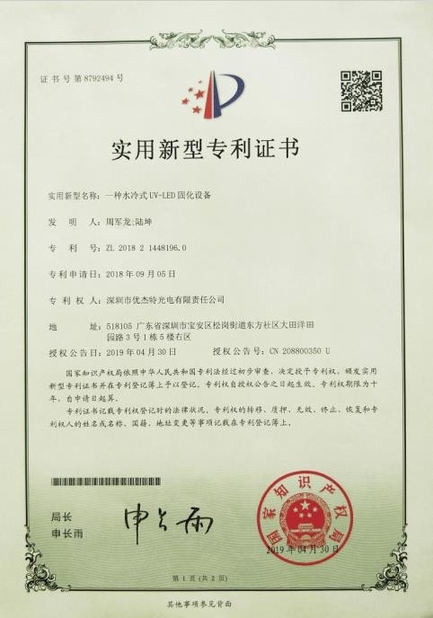
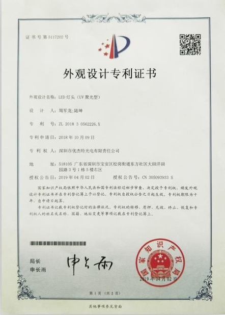
High-Yield & Low-Thermal Impact: UV-LED Curing Solutions Cover Full Lamination to OLED Encapsulation
SHANGHAI — As the global display and optoelectronic industries accelerate toward ultra-thin, flexible, and high-resolution architectures, precision manufacturing faces unprecedented challenges in process control and yield optimization. To meet the stringent demands of next-generation optical assembly, advanced industrial-grade UV-LED curing systems are setting a new technological benchmark, offering high-efficiency solutions that span from full lamination to microelectronics-level OLED encapsulation.
Traditional mercury lamp curing systems have long been a bottleneck for advanced display manufacturing due to high thermal radiation, spectral instability, and high energy consumption. Excessive heat generated during curing often leads to substrate deformation, yellowing, and optical stress, particularly in heat-sensitive materials such as OLED panels, touch sensors, and flexible printed circuits (FPCs).
The latest generation of precision UV-LED curing solutions directly addresses these pain points by combining narrow-band wavelength control with advanced thermal management. Operating with cold light sources, these systems restrict substrate surface temperature rise to under 3°C, eliminating thermal damage while maintaining consistent, high-irradiance output.
Comprehensive Coverage Across Display Manufacturing
The integration of high-precision UV-LED curing equipment with specialized optical adhesives has demonstrated significant performance gains across four critical production stages:
Liquid Optical Clear Adhesive (LOCA) Bonding: High-uniformity (>95%) UV-LED surface light source systems deliver precise gradient energy, eliminating internal stress and bubble rebound to achieve optical transmittance exceeding 99%.
Full Lamination for Large & Automotive Displays: Water-cooled UV-LED conveyor tunnels provide deep, uniform curing for large touch panels without thermal warping, ensuring long-term durability and weather resistance under harsh operating conditions.
Temporary Protection with UV Peelable Blue Masks: High-irradiance line light sources enable millisecond-level surface drying for circuit board masking. The monochromatic light prevents over-curing, allowing clean, residue-free peeling while cutting energy consumption by over 70% compared to thermal drying.
OLED & Micro-OLED Hermetic Encapsulation: Precision optical fiber spot and line light sources deliver micron-level spot control with near-zero heat transfer. This achieves ultra-tight moisture and oxygen barrier seals, protecting sensitive organic layers and maximizing packaging yield rates.
Driving Efficiency and Sustainability
Beyond yield improvements, the transition to UV-LED curing aligns with global industrial sustainability goals. Featuring instant ON/OFF capabilities, elimination of ozone emissions, and a operating lifespan exceeding 20,000 hours, UV-LED systems significantly lower total cost of ownership (TCO) for display manufacturers.
As flexible displays and micro-display technologies continue to expand into consumer electronics, automotive interiors, and wearable devices, high-precision, low-thermal UV-LED curing systems are positioned to remain a fundamental driver of high-yield, energy-efficient optoelectronic manufacturing.
Personne à contacter: Mr. Eric Hu
Téléphone: 0086-13510152819